¶ Introduction
Banana Pi BPI-SM9 16-ENC-A3 deep learning computing module is equipped with the highly integrated computing technology processor BM1688 8 Core ARM CA53 1.6GHz, 8GB LPDDR4,32GB eMMC onboard. It has 1 RJ45 Gigabit network port, 1 M.2 Key E, 1 M.2 Key M, 4 USB3.2 ports, 1 TYPE C (USB3.0) and multiple functional interfaces.
¶ Specifications
-
Supports HDMI 2.0 output;
-
Supports dual gigabit RJ45 Ethernet;
-
Supports dual-layer USB3.0 interfaces;
-
Supports dual-layer WIFI_BT function;
-
Supports TF card or M.2 SSD expansion;
-
Supports 2 MIPI camera inputs;
-
Supports expansion of GPIO;
-
Supports CAN function;
-
Supports USB-C interface upgrade (NVIDVI core board solution);
¶ Development
¶ Prepare
-
12V/3A power adapter(The voltage range is between 11 and 13 volts. Using a 12V power adapter is the most suitable option.)
-
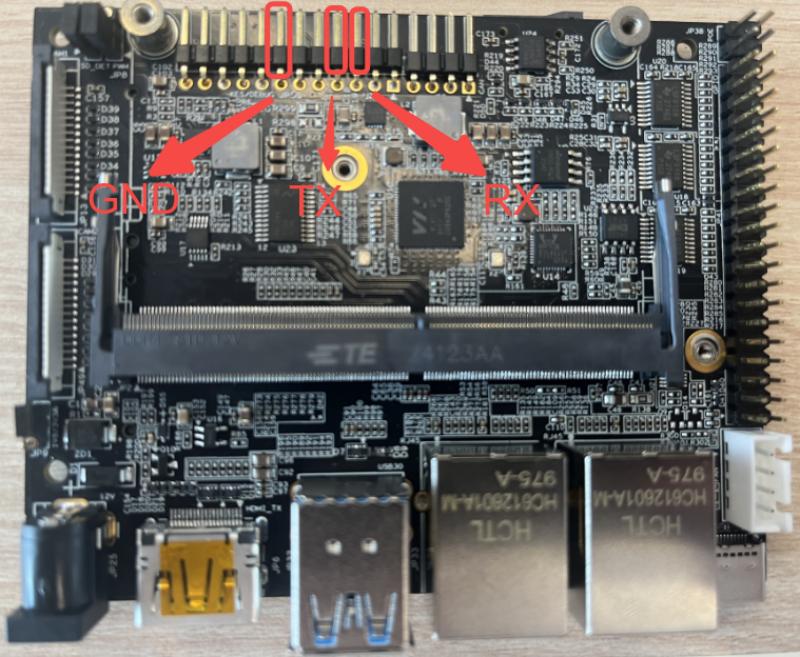
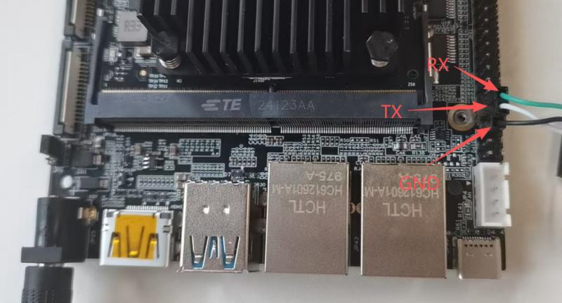
Using your USB-Serial cable(3.3V TTL,Baud=115200) Connect to debug console on BPI-SM9
-
One TF card(If you want to use the FT card for system startup)
-
One Type-C cable (for upgrade programming)
¶ tool
Baidu cloud: https://pan.baidu.com/s/1_aP12DUw99F8WNFdFH0kXg?pwd=8888 (pincode: 8888)
¶ TTL Debugport
¶ Jumper caps and the function
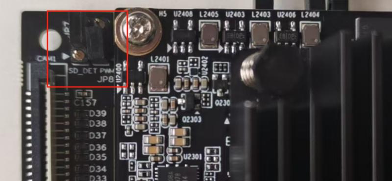
BPI-SM9 TF jumper cap and BPI-SM9 PWM control jumper cap
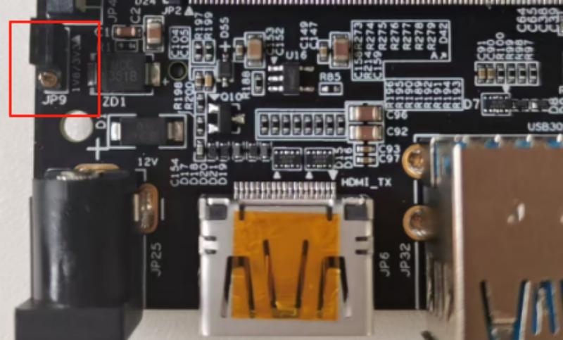
HDMI_DDC Voltage Connector jumper Cap
¶ TF card detection and GPIO selection
| JP7 jumper instructions: (For BM1688) 1. Default connection: PIN2 and PIN3, used for enabling control of the WIFI module in the BM1688/NVIDIA module; 2. When using the TF card function of BM1688, the jumper of PIN1 and PIN2 is required, used for detecting the insertion of the TF card in BM1688; |
| BPI-SM9 TF jumper pins | ||||
|---|---|---|---|---|
Numbering position |
PIN |
PIN Definition |
PIN Explanation |
Level |
JP7 |
1 |
SDMMC_DET |
TF card insertion detection |
1V8 |
2 |
GPIOC0-SDMMC_DET |
TF card insertion detection or universal GPIO |
1V8 |
|
3 |
W_DISABLE1_CTRL |
The WIFI enable control signal of the WiFi_BT module |
1V8 |
|
¶ PWM control jumper cap
| This jumper cap is used for PWM control of the FANs in different modules. By default, using the BM1688 module is sufficient. |
| BPI-SM9 PWM control jumper pins | ||||
|---|---|---|---|---|
Numbering position |
PIN |
PIN Definition |
PIN Explanation |
Level |
JP8 |
1 |
BM1688_FAN_PWM5 |
The PWM control pin of BM1688 |
1V8 |
2 |
FAN_PWM |
The PWM control input of FAN |
1V8 |
|
3 |
NVIDIA_FAN_PWM |
NVIDIA’s PWM control pin |
1V8 |
|
¶ HDMI_DDC Voltage Connector jumper Cap
| For the level selection of different modules, here it is assumed that 1.8V can be used. |
| BPI-SM9 HDMI_DDC Voltage Connector jumper pins | ||||
|---|---|---|---|---|
Numbering position |
PIN |
PIN Definition |
PIN Explanation |
Level |
JP8 |
1 |
1V8 |
Power supply 1.8V |
1V8 |
2 |
VDD_DDC |
The power supply options of DDC |
1V8 / 3V3 |
|
3 |
3V3 |
Power supply 3.3V |
3V3 |
|
¶ Accessories
¶ SD card burn image
| Please pay attention to whether the TF card clips on the board are correctly positioned. please see: TF card detection and GPIO selection |
-
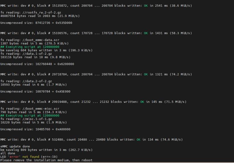
First, download the corresponding SD card burning package, and then copy the files in it to the SD card.
-
Insert the card into the BPI-SM9 and power it on to start.
-
Finally, it will automatically be updated and burned.
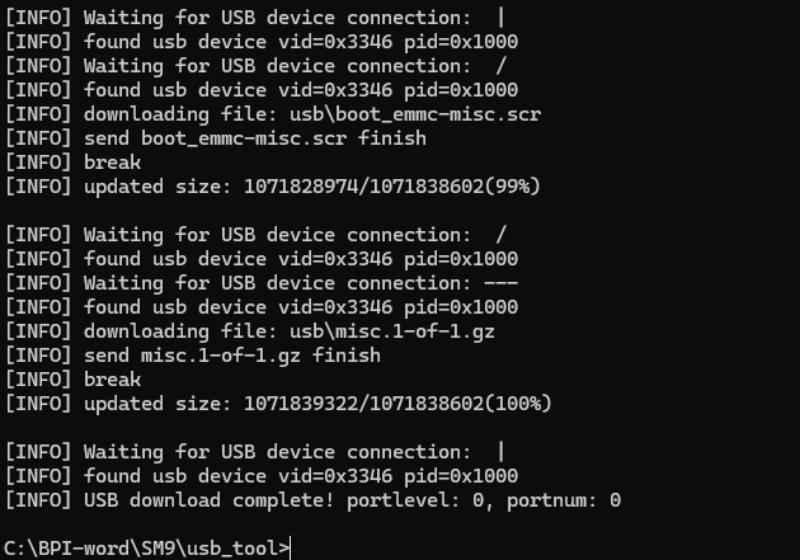
¶ OTG typeC burn image
-
Please download and unzip the tool flashing package "usb_tool".
-
Double-click on CviUsbInstallDriver.exe to install the driver for your PC.
-
Open the Windows Command Prompt in the directory of the usb_dl.exe file and enter:
./usb_dl.exe -c cv186x -i usb\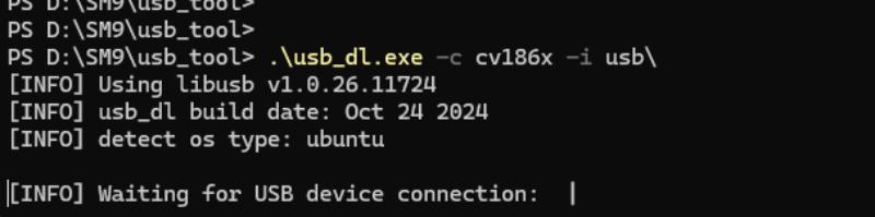
-
When the above interface appears, simply reinsert and remove the OTG type C interface to proceed with the burning process.
¶ USB3.0
admin@sophon:~$ lsblk
NAME         MAJ:MIN RM  SIZE RO TYPE MOUNTPOINTS
sda            8:0    1 14.8G  0 disk
└─sda1         8:1    1 14.8G  0 part /media/storage-hot-sda1
mmcblk0      179:0    0 28.9G  0 disk
├─mmcblk0p1  179:1    0  128M  0 part /boot
├─mmcblk0p2  179:2    0  128M  0 part /recovery
├─mmcblk0p3  179:3    0   10M  0 part
├─mmcblk0p4  179:4    0    7G  0 part /media/root-ro
├─mmcblk0p5  179:5    0    7G  0 part /media/root-rw
└─mmcblk0p6  179:6    0    4G  0 part /data
mmcblk0boot0 179:8    0    4M  1 disk
mmcblk0boot1 179:16 0 4M 1 disk¶ Uart1
¶ send
Use script to send
admin@sophon:~/storage-hot-sda1$ cat uart_send.sh
#!/bin/bash

# 检查传入的参数数量是否正确
if [ $# -ne 2 ]; then
    echo "用法: $0 <串口设备名称> <波特率>"
    echo "示例: $0 /dev/ttyS1 9600"
    exit 1
fi

# 获取传入的串口设备名称和波特率
serial_device=$1
baud_rate=$2

# 配置串口设备
sudo stty -F $serial_device $baud_rate raw

# 要发送的数据
data="hello, hdzk!\r\n"

# 无限循环发送数据
while true; do
    echo -e "$data" | sudo tee $serial_device > /dev/null
    if [ $? -ne 0 ]; then
        echo "数据发送失败。"
        break
    fi
    sleep 1
done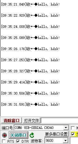
¶ receive
Use script to receive
admin@sophon:~/storage-hot-sda1$ cat uart_send.sh
#!/bin/bash

# 检查传入的参数数量是否正确
if [ $# -ne 2 ]; then
    echo "用法: $0 <串口设备名称> <波特率>"
    echo "示例: $0 /dev/ttyS1 9600"
    exit 1
fi

# 获取传入的串口设备名称和波特率
serial_device=$1
baud_rate=$2

# 配置串口设备
sudo stty -F $serial_device $baud_rate raw

# 要发送的数据
data="hello, hdzk!\r\n"

# 无限循环发送数据
while true; do
    echo -e "$data" | sudo tee $serial_device > /dev/null
    if [ $? -ne 0 ]; then
        echo "数据发送失败。"
        break
    fi
    sleep 1
doneReceived on the board
admin@sophon:~/storage-hot-sda1$ ./uart_receive.sh /dev/ttyS1 9600
123hello▒▒testhello▒▒testhello
testhello
testhello
testhello
test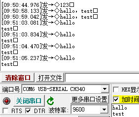
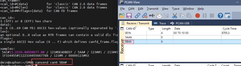
¶ CAN
| blue :CAN_H Green: CAN_L |
Connection interface
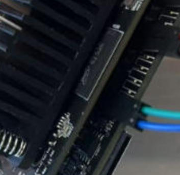
CAN communication can be easily implemented using the scripts in the SM9 folder.
¶ eth interface
| The eth0 interface is located near the type-c interface.The other one is the eth1 interface. |
| The default static IP address for the eth1 network interface mirror is 192.168.150.1.You can modify the IP address in /etc/netplan/01-netcfg.yaml |
Connect the network port to the computer using a network cable.
¶ eth0
-
Use the command to set the IP address of eth0.
sudo ifconfig eth0 xxx(xxx is ip)iperf3 test speed
¶ M.2 KeyE
Supported network cards: Intel RTL8822CE
¶ WiFi STA
| You can modify the WiFi username and password you want to connect to in /etc/wpa_supplicant.conf |
-
First, execute the command to add the WiFi driver.
sudo insmod /mnt/system/ko/3rd/xxx.ko //xxx is the network cards name -
Connect to WiFi using a script
./wifista.sh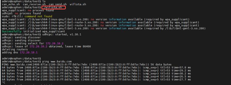
¶ WiFi AP
| You can modify the WiFi username and password to be created in /etc/hostapd.conf |
If you have already loaded the driver in your system, you can directly execute the script to create a Wi-Fi network.
./wifiap.sh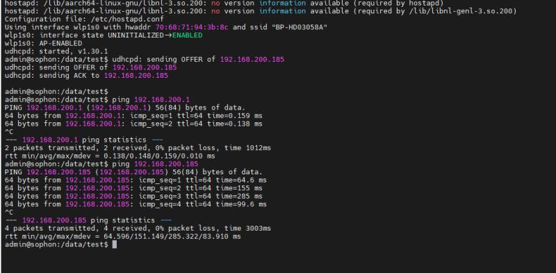
¶ bluetooth
-
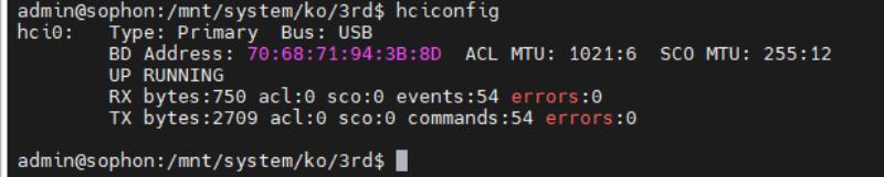
Load driver: sudo insmod /mnt/system/ko/3rd/rtk_btusb.ko
-
Verify driver functionality, use
hciconfigIf a Bluetooth node is present, the driver is functioning correctly.
-
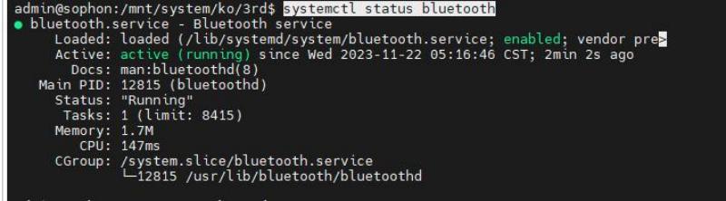
Confirm Bluetooth service is running normally
-
Use BlueZ tools for communication
bluetoothctl  //Enter Bluetooth debugging tool
power on      //Turn on Bluetooth power
scan on       //Scan for surrounding Bluetooth
pair XX:XX:XX:XX:XX:XX   //Connect via Bluetooth (The following is MAC address)
¶ RTC
Please install a CR1220 button battery in the SM9 before use.
-
View the current clock use the command:
sudo hwclock -r --show -
Set the clock:
sudo date -s "20xx-xx-xx 09:09:55" -
Synchronize to hardware clock:
sudo hwclock --systohc -
Power off and restart, then check the clock:
sudo hwclock -r --show -
It can be determined that the displayed time is an RTC clock.
¶ NVME
Connect NVMe to the M.2 SSD interface.Then you can use this hard drive.
¶ CAMERA
| They cannot be used simultaneously. |
¶ CAM1
| Near the JP7 |
If you are using a different MIPI camera, please uninstall the driver for that camera first:
rmmod /mnt/system/ko/v4l2_csi0_ov5647.ko
-
Switch I2C to csi2:
echo 8 > /proc/zkwl/gpio -
Install driver:
sudo insmod /mnt/system/ko/v4l2_csi2_ov5647.ko -
Create a video stream:
cd /opt/sophon/sophon-soc-libisp-dev_1.0.0/bin/sudo ./CviIspTool.sh -
Use your video software to pull the video stream from VLC.
¶ CAM2
| Near the 12V power port |
If you are using a different MIPI camera, please uninstall the driver for that camera first:
rmmod /mnt/system/ko/v4l2_csi2_ov5647.ko
-
Switch I2C to csi0:
echo 9 > /proc/zkwl/gpio -
Install driver:
sudo insmod /mnt/system/ko/v4l2_csi0_ov5647.ko -
Create video stream length
cd /opt/sophon/sophon-soc-libisp-dev_1.0.0/bin/sudo ./CviIspTool.sh -
. Use your video software to pull the video stream from VLC.
¶ GPIO Define
¶ 260PIN Gold Finger interface
Details
| BPI-SM9 260PIN Gold Finger interface | |||||
|---|---|---|---|---|---|
BPI-SM9-CON |
PIN |
Level |
Level |
PIN |
BPI-SM9-CON |
GND |
1 |
/ |
/ |
2 |
GND |
CSI1_D0_N |
3 |
1V8 |
1V8 |
4 |
CSI0_D0_N |
CSI1_D0_P |
5 |
1V8 |
1V8 |
6 |
CSI0_D0_P |
GND |
7 |
/ |
/ |
8 |
GND |
CSI1_CLK_N |
9 |
1V8 |
1V8 |
10 |
CSI0_CLK_N |
CSI1_CLK_P |
11 |
1V8 |
1V8 |
12 |
CSI0_CLK_P |
GND |
13 |
/ |
/ |
14 |
GND |
CSI1_D1_N |
15 |
1V8 |
1V8 |
16 |
CSI0_D1_N |
CSI1_D1_P |
17 |
1V8 |
1V8 |
18 |
CSI0_D1_P |
GND |
19 |
/ |
/ |
20 |
GND |
CSI3_D0_N |
21 |
1V8 |
1V8 |
22 |
CSI2_D0_N |
CSI3_D0_P |
23 |
1V8 |
1V8 |
24 |
CSI2_D0_P |
GND |
25 |
/ |
/ |
26 |
GND |
CSI3_CLK_N |
27 |
1V8 |
1V8 |
28 |
CSI2_CLK_N |
CSI3_CLK_P |
29 |
1V8 |
1V8 |
30 |
CSI2_CLK_P |
GND |
31 |
/ |
/ |
32 |
GND |
CSI3_D1_N |
33 |
1V8 |
1V8 |
34 |
CSI2_D1_N |
CSI3_D1_P |
35 |
1V8 |
1V8 |
36 |
CSI2_D1_P |
GND |
37 |
/ |
/ |
38 |
GND |
USBSS1_RX_N |
39 |
3V3 |
1V8 |
40 |
I_VDD_IN |
USBSS1_RX_P |
41 |
3V3 |
3V3 |
42 |
TEMP_ALR_N(GPIO130) |
GND |
43 |
/ |
/ |
44 |
GND |
USBSS1_TX_N |
45 |
3V3 |
1V8 |
46 |
CSI5_CLK_N |
USBSS1_TX_P |
47 |
3V3 |
1V8 |
48 |
CSI5_CLK_P |
GND |
49 |
/ |
/ |
50 |
GND |
CSI5_D0_N |
51 |
1V8 |
1V8 |
52 |
RGMII1_RXD0 |
CSI5_D0_P |
53 |
1V8 |
1V8 |
54 |
RGMII1_RXD1 |
GND |
55 |
/ |
/ |
56 |
GND |
CSI5_D1_N |
57 |
1V8 |
1V8 |
58 |
RGMII1_RXD2 |
CSI5_D1_P |
59 |
1V8 |
1V8 |
60 |
RGMII1_RXD3 |
GND |
61 |
/ |
/ |
62 |
GND |
HDMI_N2 |
63 |
/ |
1V8 |
64 |
RGMII1_RXC |
HDMI_P2 |
65 |
/ |
1V8 |
66 |
RGMII1_RXCTRL |
GND |
67 |
/ |
/ |
68 |
GND |
HDMI_N1 |
69 |
/ |
1V8 |
70 |
RGMII1_TXD0 |
HDMI_P1 |
71 |
/ |
1V8 |
72 |
RGMII1_TXD1 |
GND |
73 |
/ |
/ |
74 |
GND |
HDMI_N0 |
75 |
/ |
1V8 |
76 |
RGMII1_TXD2 |
HDMI_P0 |
77 |
/ |
1V8 |
78 |
RGMII1_TXD3 |
GND |
79 |
/ |
/ |
80 |
GND |
HDMI_CLKN |
81 |
/ |
/ |
82 |
RGMII1_TXC |
HDMI_CLKP |
83 |
/ |
/ |
84 |
RGMII1_TXCTRL |
GND |
85 |
3V3 |
1V8 |
86 |
GND |
PWR_GPIO14 |
87 |
1V8 |
1V8 |
88 |
I2S1_DOUT |
SPI3_MOSI |
89 |
1V8 |
1V8 |
90 |
I2S1_DIN |
SPI3_SCK |
91 |
1V8 |
1V8 |
92 |
I2S1_FS |
SPI3_MISO |
93 |
1V8 |
1V8 |
94 |
I2S2_MCLK |
SPI3_CS0* |
95 |
1V8 |
1V8 |
96 |
HDMI_HPD |
SPI3_CS1* |
97 |
1V8 |
1V8 |
98 |
HDMI_DDC_SDA |
UART4_TXD |
99 |
1V8 |
1V8 |
100 |
HDMI_DDC_SCL |
UART4_RXD |
101 |
1V8 |
/ |
102 |
GND |
UART4_RTS |
103 |
1V8 |
1V8 |
104 |
SPI1_MOSI |
UART4_CTS |
105 |
1V8 |
1V8 |
106 |
SPI1_SCK |
GND |
107 |
/ |
1V8 |
108 |
SPI1_MISO |
USB0_D_N |
109 |
3V3 |
1V8 |
110 |
SPI1_CS0* |
USB0_D_P |
111 |
3V3 |
1V8 |
112 |
SPI1_CS1* |
GND |
113 |
/ |
1V8 |
114 |
CAM0_PWDN |
USB1_D_N |
115 |
3V3 |
1V8 |
116 |
CAM0_MCLK |
USB1_D_P |
117 |
3V3 |
1V8 |
118 |
GPIO01/I2S0_MCLK |
GND |
119 |
/ |
1V8 |
120 |
CAM1_PWDN |
CAM2_MCLK |
121 |
1V8 |
1V8 |
122 |
CAM1_MCLK |
CAM3_MCLK |
123 |
1V8 |
1V8 |
124 |
PWR_GPIO17 |
GND |
125 |
/ |
1V8 |
126 |
GPIO61 |
GPIO68 |
127 |
1V8 |
1V8 |
128 |
GPIO05/SD_CD |
GND |
129 |
/ |
1V8 |
130 |
GPIO60/SD0_PWR_E N |
PCIE1_RX0_N |
131 |
1V8 |
/ |
132 |
GND |
PCIE1_RX0_P |
133 |
1V8 |
1V8 |
134 |
PCIE1_TX0_N |
GND |
135 |
/ |
1V8 |
136 |
PCIE1_TX0_P |
PCIE1_RX1_N |
137 |
1V8 |
/ |
138 |
GND |
PCIE1_RX1_P |
139 |
1V8 |
1V8 |
140 |
PCIE1_TX1_N |
GND |
141 |
/ |
1V8 |
142 |
PCIE1_TX1_P |
CAN0_RX |
143 |
3V3 |
/ |
144 |
GND |
CAN0_TX |
145 |
3V3 |
/ |
146 |
GND |
GND |
147 |
/ |
1V8 |
148 |
I2S2_FS |
I2S2_DOUT |
149 |
1V8 |
1V8 |
150 |
I2S2_SCLK |
I2S2_DIN |
151 |
1V8 |
/ |
152 |
GND |
GND |
153 |
/ |
1V8 |
154 |
PCIE0_TX1_N |
PCIE0_RX1_N |
155 |
1V8 |
1V8 |
156 |
PCIE0_TX1_P |
PCIE0_RX1_R |
157 |
1V8 |
/ |
158 |
GND |
GND |
159 |
/ |
1V8 |
160 |
PCIE1_EP_CLK_N |
USBSS0_RX_N |
161 |
3V3 |
1V8 |
162 |
PCIE1_EP_CLK_P |
USBSS0_RX_P |
163 |
3V3 |
/ |
164 |
GND |
GND |
165 |
/ |
3V3 |
166 |
USBSS0_TX_N |
PCIE0_RX0_N |
167 |
1V8 |
3V3 |
168 |
USBSS0_TX_P |
PCIE0_RX0_P |
169 |
1V8 |
/ |
170 |
GND |
GND |
171 |
/ |
1V8 |
172 |
PCIE0_TX0_N |
PCIE0_EP_CLK_N |
173 |
1V8 |
1V8 |
174 |
PCIE0_TX0_P |
PCIE0_EP_CLK_P |
175 |
1V8 |
/ |
176 |
GND |
GND |
177 |
/ |
1V8 |
178 |
MOD_SLEEP* |
PCIE_WAKE* |
179 |
3V3 |
3V3 |
180 |
PCIE1_CLKREQ* |
PCIE1_RST* |
181 |
3V3 |
3V3 |
182 |
PCIE0_CLKREQ* |
PCIE0_RST* |
183 |
3V3 |
/ |
184 |
GBE0_MDI0_N |
I2C4_SCL |
185 |
3V3 |
/ |
186 |
GBE0_MDI0_P |
I2C4_SDA |
187 |
3V3 |
3V3 |
188 |
PHY0_CFG_LDO0/PH Y0_CFG_EXT |
I2C5_SCL |
189 |
3V3 |
/ |
190 |
GBE0_MDI1_N |
I2C5_SDA |
191 |
3V3 |
/ |
192 |
GBE0_MDI1_P |
I2S0_DOUT |
193 |
1V8 |
3V3 |
194 |
PHY0_CFG_LDO1 |
I2S0_DIN |
195 |
1V8 |
/ |
196 |
GBE0_MDI2_N |
I2S0_FS |
197 |
1V8 |
/ |
198 |
GBE0_MDI2_P |
I2S0_SCLK |
199 |
1V8 |
/ |
200 |
GND |
GND |
201 |
/ |
/ |
202 |
GBE0_MDI3_N |
UART1_TXD |
203 |
/ |
/ |
204 |
GBE0_MDI3_P |
UART1_RXD |
205 |
1V8 |
1V8 |
206 |
GPIO79 |
UART1_RTS* |
207 |
1V8 |
1V8 |
208 |
PWR_GPIO16 |
UART1_CTS* |
209 |
1V8 |
3V3 |
210 |
CLK_32K_OUT |
GPIO09/I2S1_MCLK |
211 |
1V8 |
1V8 |
212 |
GPIO100 |
CAM_I2C_SCL |
213 |
3V3 |
1V8 |
214 |
FORCE_RECOVERY* |
CAM_I2C_SDA |
215 |
3V3 |
1V8 |
216 |
GPIO99 |
MODULE_ID |
217 |
1V8 |
1V8 |
218 |
GPIO80 |
SDMMC_DAT0 |
219 |
3V3 |
1V8 |
220 |
RGMII1_MDC |
SDMMC_DAT1 |
221 |
3V3 |
1V8 |
222 |
RGMII1_MDIO |
SDMMC_DAT2 |
223 |
3V3 |
1V8 |
224 |
PHY1_RGMII_IRQ |
SDMMC_DAT3 |
225 |
3V3 |
1V8 |
226 |
I2S1_SCLK |
SDMMC_CMD |
227 |
3V3 |
1V8 |
228 |
GPIO98 |
SDMMC_CLK |
229 |
3V3 |
1V8 |
230 |
GPIO97 |
GND |
231 |
/ |
1V8 |
232 |
I2C3_SCL |
SHUTDOWN_REQ* |
233 |
5V |
1V8 |
234 |
I2C3_SDA |
PMIC_BBAT |
235 |
3V3 |
1V8 |
236 |
UART0_TXD |
POWER_EN |
237 |
5V |
1V8 |
238 |
UART0_RXD |
MODULE_RESET |
239 |
1V8 |
5V |
240 |
SLEEP/WAKE* |
GND |
241 |
/ |
/ |
242 |
GND |
GND |
243 |
/ |
/ |
244 |
GND |
GND |
245 |
/ |
/ |
246 |
GND |
GND |
247 |
/ |
/ |
248 |
GND |
GND |
249 |
/ |
/ |
250 |
GND |
VDD_IN |
251 |
5V |
5V |
252 |
VDD_IN |
VDD_IN |
253 |
5V |
5V |
254 |
VDD_IN |
VDD_IN |
255 |
5V |
5V |
256 |
VDD_IN |
VDD_IN |
257 |
5V |
5V |
258 |
VDD_IN |
VDD_IN |
259 |
5V |
5V |
260 |
VDD_IN |
¶ 40-pin interface
| The default level of the 40-pin GPIO is 3.3V (except for the 5V pin) |
Details
| BPI-SM9 40 PIN Header GPIO define of JP41 | |||
|---|---|---|---|
BPI-SM9-CON |
PIN |
PIN |
BPI-SM9-CON |
5V |
1 |
2 |
3V3 |
5V |
3 |
4 |
I2C1_SDA |
GND |
5 |
6 |
I2C1_SCL |
UART1_TXD |
7 |
8 |
GPIO09 |
UART1_RXD |
9 |
10 |
GND |
I2S0_SCLK |
11 |
12 |
UART1_RTS |
GND |
13 |
14 |
SPI1_SCK |
SPI1_CS1 |
15 |
16 |
GPIO12 |
SPI1_CS0 |
17 |
18 |
3V3 |
GND |
19 |
20 |
SPI0_MOSI |
SPI1_MISO |
21 |
22 |
SPI0_MISO |
SPI0_CS0 |
23 |
24 |
SPI0_SCK |
SPI0_CS1 |
25 |
26 |
GND |
ID_I2C_SCL |
27 |
28 |
ID_I2C_SDA |
GND |
29 |
30 |
GPIO01 |
GPIO07 |
31 |
32 |
GPIO11 |
GND |
33 |
34 |
GPIO13 |
UART1_CTS |
35 |
36 |
I2S0_LRCK |
I2S0_SDIN |
37 |
38 |
SPI1_MOSI |
I2S0_SDOUT |
39 |
40 |
GND |
¶ Fan control interface
Details
| BPI-SM9 Fan control interface of JP4 | ||
|---|---|---|
PIN |
Definition |
Level |
1 |
GND |
/ |
2 |
12V |
12V |
3 |
TACH |
5V |
4 |
PWM |
5V |
¶ POE interface
Details
| BPI-SM9 POE interface of JP38 | ||
|---|---|---|
PIN |
Definition |
Level |
1 |
POE_VC2 |
/ |
2 |
POE_VC1 |
/ |
3 |
POE_VC4 |
/ |
4 |
POE_VC3 |
/ |
¶ CANH/L interface
Details
| BPI-SM9 CANH/L interface of JP5 | ||
|---|---|---|
PIN |
Definition |
Level |
1 |
CANH |
3V3 |
2 |
CANL |
3V3 |
3 |
GND |
/ |
4 |
3V3 |
3V3 |
¶ 12-pin interface
Details
| BPI-SM9 12-pin interface of JP50 | ||
|---|---|---|
PIN |
Definition |
Level |
1 |
PC_LED- |
5V |
2 |
PC_LED+ |
5V |
3 |
UART2_RX |
3V3 |
4 |
UART2_TX |
3V3 |
5 |
LATCH_SET |
5V |
6 |
LATCH_SET_BUT |
5V |
7 |
GND |
/ |
8 |
SYS_RST |
1V8 |
9 |
GND |
/ |
10 |
FORCE_RECOVERY |
1V8 |
11 |
GND |
/ |
12 |
PWR_BTN |
5V |
¶ Camera interface
¶ Camera1
Details
| BPI-SM9 Camera1 of JP13 | ||
|---|---|---|
PIN |
Definition |
Level |
1 |
GND |
/ |
2 |
NC |
/ |
3 |
CSI2_D0_N |
1V8 |
4 |
NC |
/ |
5 |
CSI2_D0_P |
1V8 |
6 |
NC |
/ |
7 |
GND |
/ |
8 |
NC |
/ |
9 |
CSI2_D1_N |
1V8 |
10 |
NC |
1V8 |
11 |
CSI2_D1_P |
1V8 |
12 |
NC |
/ |
13 |
GND |
/ |
14 |
NC |
/ |
15 |
CSI2_CLK_N |
1V8 |
16 |
NC |
/ |
17 |
CSI2_CLK_P |
1V8 |
18 |
NC |
/ |
19 |
GND |
/ |
20 |
NC |
/ |
21 |
CAM1_PWDN |
1V8 |
22 |
NC |
/ |
23 |
CAM1_MCLK |
1V8 |
24 |
NC |
/ |
25 |
CAM1_I2C_SCL |
3V3 |
26 |
NC |
/ |
27 |
CAM1_I2C_SDA |
3V3 |
28 |
NC |
/ |
29 |
3V3 |
3V3 |
30 |
NC |
/ |
¶ Camera2
Details
| BPI-SM9 Camera2 of JP49 | ||
|---|---|---|
PIN |
Definition |
Level |
1 |
GND |
/ |
2 |
NC |
/ |
3 |
CSI0_D0_N |
1V8 |
4 |
NC |
/ |
5 |
CSI0_D0_P |
1V8 |
6 |
NC |
/ |
7 |
GND |
/ |
8 |
NC |
/ |
9 |
CSI0_D1_N |
1V8 |
10 |
NC |
1V8 |
11 |
CSI0_D1_P |
1V8 |
12 |
NC |
/ |
13 |
GND |
/ |
14 |
NC |
/ |
15 |
CSI0_CLK_N |
1V8 |
16 |
NC |
/ |
17 |
CSI0_CLK_P |
1V8 |
18 |
NC |
/ |
19 |
GND |
/ |
20 |
NC |
/ |
21 |
CAM0_PWDN |
1V8 |
22 |
NC |
/ |
23 |
CAM0_MCLK |
1V8 |
24 |
NC |
/ |
25 |
CAM0_I2C_SCL |
3V3 |
26 |
NC |
/ |
27 |
CAM0_I2C_SDA |
3V3 |
28 |
NC |
/ |
29 |
3V3 |
3V3 |
30 |
NC |
/ |